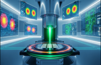
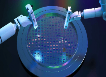
In a development that could transform nondestructive testing (NDT) in semiconductor manufacturing, Kioxia Iwate Corporation is set to begin evaluating a GaN (Gallium Nitride)-based electron beam (e-Beam) inspection and metrology technology later this month.
The system, jointly developed by Nagoya University startup Photo electron Soul Inc. (PeS) and the Amano-Honda Laboratory at Nagoya University, will undergo field testing to validate its potential for advanced 3D NAND flash memory production. The evaluation will focus on enhancing defect identification and root-cause analysis in live production environments, a critical need as device structures grow increasingly complex.
Why e-Beam Matters for NDT in Semiconductors
Electron beam inspection is regarded as one of the most advanced nondestructive testing techniques for semiconductors. Unlike traditional optical or mechanical methods, e-Beam systems provide ultra-high-resolution images by directing electrons onto a wafer and analyzing the scattered signals. This enables detection of surface defects, cracks, voids, and even subsurface anomalies without damaging fragile structures.
However, conventional e-Beam systems face throughput limitations, often restricting their use to sampling inspections rather than production-scale monitoring. The GaN-based photocathode technology developed by PeS and Nagoya University is designed to address this challenge by delivering both high precision and improved speed.
The GaN-Based Breakthrough
At the heart of the innovation are GaN-based photocathodes, which enable efficient electron emission and more precise beam control. This advancement supports two novel modes:
- DSeB (Digital Selective e-Beaming): Targeted e-Beam radiation for selective inspection.
- YCeB (Yield Controlled e-Beaming): Real-time beam intensity control for accuracy and consistency.
Together, these innovations overcome the long-standing throughput and precision trade-offs in e-Beam inspection, bringing the possibility of true production-scale deployment.
A Step Toward Commercialization
Takayuki Suzuki, CEO of PeS, highlighted the significance of the evaluation:
“This evaluation provides a great opportunity for us to prove that our inspection and metrology technology is unmatched. No other inspection tool supplier has yet commercialized it, and it is ready for production in a semiconductor manufacturing environment.”
He added, “We are confident that this will become a core technology for Kioxia, enabling them to significantly enhance their advanced inspection and metrology capabilities and outperform rival NAND flash producers in Korea and the US.”
Implications for NDT and Beyond
If successful, the technology could redefine nondestructive defect detection in 3D NAND flash manufacturing and potentially extend into other advanced semiconductor devices. By combining the precision of e-Beam inspection with production-level throughput, this breakthrough directly addresses one of the semiconductor industry’s most pressing challenges—maintaining yield while scaling complexity.
For NDT in semiconductors, the GaN-based photocathode e-Beam system may mark the beginning of a new era where electron beam inspection evolves from a sampling tool into a mainstream production enabler.


