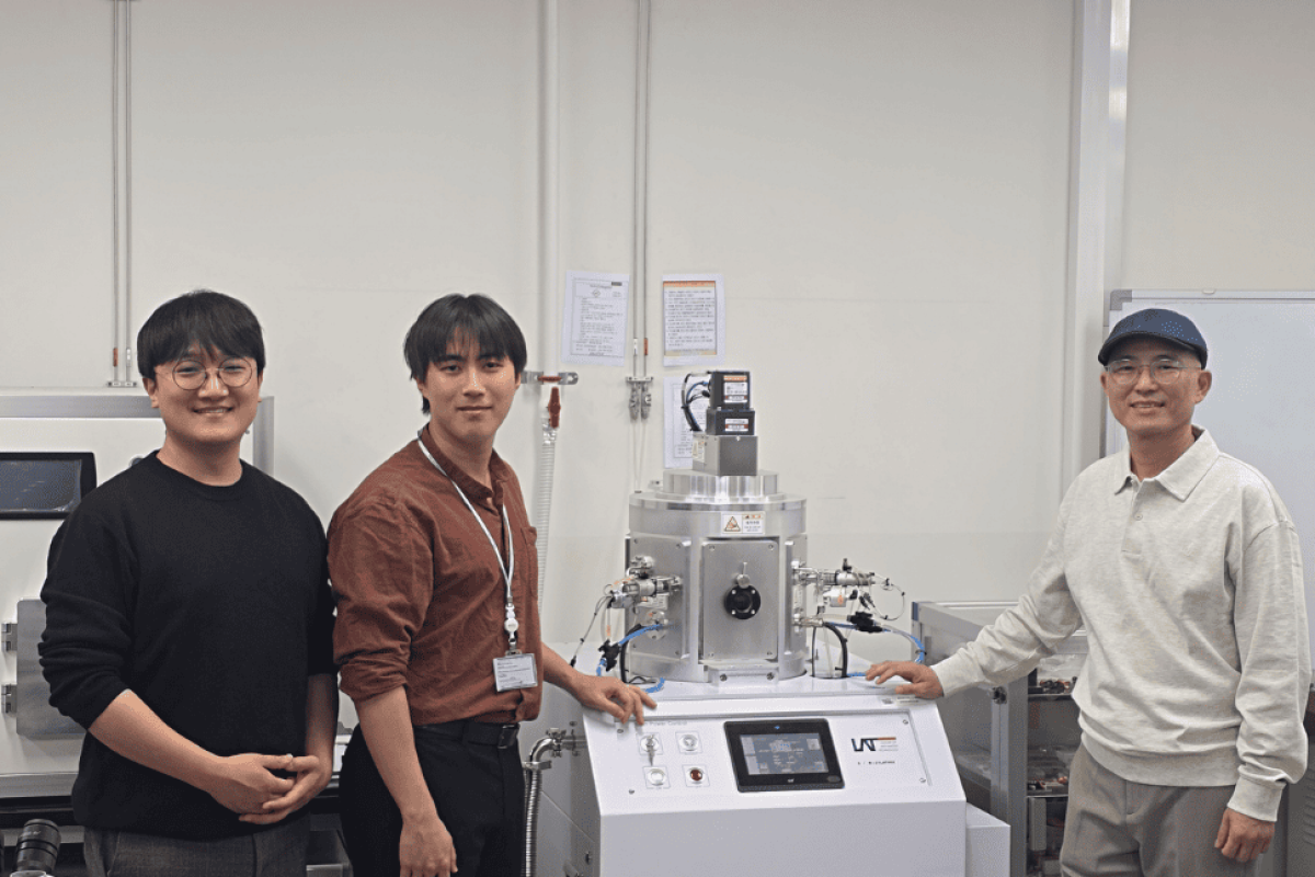
Researchers at Daegu Gyeongbuk Institute of Science and Technology (DGIST), South Korea, have developed a screw-lens-focused ultrasonic transducer designed to improve the detection of micro-defects inside semiconductor chips. The technology reduces internal ultrasonic noise by introducing a threaded structure on the side surface of the transducer lens, enabling clearer imaging without increasing the sensor's overall size.
The research was led by Professor Chang Jin Ho from DGIST’s Department of Electrical, Electronic and Computer Science. The development could support non-destructive testing (NDT) of high-reliability power semiconductors used in electric vehicles and aerospace applications, where detecting microscopic defects is critical to component performance and reliability.
Screw-Lens Design Addresses Internal Ultrasonic Noise
Ultrasonic testing is widely used to inspect semiconductor components for internal defects such as micro-cracks and voids without damaging the devices. Compared with optical inspection and X-ray methods, ultrasound offers strong penetration capabilities for examining internal structures.
Industrial semiconductor inspection systems commonly use a water-column transmission technique, also known as the waterfall method. However, limitations on sensor size can make it difficult to improve image quality by simply increasing the dimensions of the lens. In compact sensors, ultrasonic waves can reflect and interfere within the lens, generating edge noise that obscures fine internal features.
To address this issue, the DGIST team drew inspiration from the angled, sound-absorbing structures used in anechoic chambers. Researchers machined slanted, screw-thread-shaped grooves into the outer side surface of the ultrasonic lens. When ultrasonic waves reach these inclined surfaces, they scatter in multiple directions rather than reflecting back and converging to produce unwanted noise.
Computer simulations helped the team identify suitable design parameters for the threaded structure, including a thread height of 500 μm and an inclination angle of 30 degrees. According to the research team, these specifications provide effective noise suppression while remaining practical to manufacture.
The design does not require changes to the sensor's overall dimensions or internal core components. Instead, the modification is made to the lens's outer surface, potentially allowing the technology to be integrated into existing compact industrial inspection equipment.
Micro-defects Visualised in Automotive Power Modules
The researchers tested the developed transducer on automotive power semiconductor modules. The new design enabled clearer visualisation of internal microstructures and defects that were difficult to distinguish using conventional ultrasonic sensors because of internal noise.
The inspection revealed fine metal wires approximately one-quarter the thickness of a human hair, along with microscopic bubbles. The resulting image clarity was reported to be comparable to that of conventional computed tomography (CT) imaging.
The development is particularly relevant to power semiconductor inspection, as these components must withstand high operating voltages and temperatures in applications such as electric vehicles and aerospace systems.
Potential for High-Frequency Ultrasonic Inspection
Professor Chang Jin Ho said the research addresses a major challenge in designing ultrasonic sensors for industrial inspection by reducing internal lens noise through a modification to the lens geometry. He added that the approach could establish a foundation for mass-producing ultra-high-frequency ultrasonic transducers operating at 100 MHz or higher.
The team plans to conduct further testing in collaboration with semiconductor manufacturers to evaluate the technology against defects encountered in actual manufacturing processes. These studies are expected to help advance NDT systems designed around industrial inspection requirements.
The research was supported by programmes from South Korea’s Ministry of Science and ICT (MSIT), the National Research Foundation of Korea and the Institute of Information & Communications Technology Planning & Evaluation (IITP). DGIST postdoctoral researcher Kang Sungwoo and integrated master’s-Ph.D. student Park Hyunkyu participated as co-first authors. The findings were published in the international journal NDT & E International.