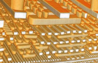
A team of researchers from the Paul Scherrer Institute, the University of Southern California, and ETH Zürich have announced a groundbreaking X-ray imaging technique capable of delivering high-resolution 3D images of computer chip interiors without the need for destructive methods. The new technology, called ptychographic X-ray laminography (PyXL), represents a significant advancement in semiconductor inspection and could greatly benefit the industry.
PyXL, which was initially capable of resolving details as small as 19 nanometers, has been further refined using a technique known as burst ptychography. This enhancement has dramatically improved the system’s resolution to an impressive 4 nanometers, allowing for detailed, non-destructive imaging of chip structures.
Traditionally, engineers have relied on destructive methods like slicing or grinding through layers of material to analyze the internal structures of computer chips, followed by examination under a transmission electron microscope (TEM). These methods, however, are not only time-consuming but also result in the loss of the chip being examined. PyXL, with its ability to produce clear and detailed 3D images, offers a non-destructive alternative that could streamline the analysis process and preserve the integrity of the chips being inspected.
Baohua Niu, a principal engineer at Intel Foundry, highlighted the potential impact of PyXL on the industry in a statement to IEEE Spectrum. Niu pointed out that prior to PyXL, engineers had to use a combination of techniques to narrow down potential problem areas on a chip before resorting to destructive methods for further analysis. This new technique, however, allows for the identification of issues within the chip without causing any damage, making it a more efficient and less risky approach.
While the resolution of PyXL is currently four to five times lower than that of a TEM, Niu emphasized the benefits of the much deeper 3D images it provides, which can reach depths of up to 5 micrometres compared to the 10 to 30-nanometer depth visible via a TEM. This depth, combined with the clarity of the images, allows for a more comprehensive understanding of the chip's structure and function, which is critical for efficient design feedback and validation processes.
The researchers demonstrated PyXL's capabilities by imaging AMD Ryzen processors manufactured using TSMC’s 7nm process node. The technology was able to reveal the intricate details of Ryzen’s FinFET transistors, including their precise placement and interconnects, offering valuable insights into the quality of chip manufacturing and engineering.
Tony Levi, a researcher at the University of Southern California, noted that PyXL could also be instrumental in identifying inconsistencies across chips, potentially offering insights into the variations that contribute to the so-called "silicon lottery." "You can figure out how good the engineering is and the manufacturing," Levi explained. "You can see the quality in one chip, the slipshod in another."
As chips continue to evolve with increasingly complex 3D architectures, the ability to obtain detailed, non-destructive 3D images will become an invaluable tool for the semiconductor industry. PyXL stands at the forefront of this technological advancement, offering a new standard for chip inspection and analysis.
https://www.tomshardware.com/tech-industry/semiconductors/researchers-detail-revolutionary-new-x-ray-tech-for-seeing-inside-computer-chips


