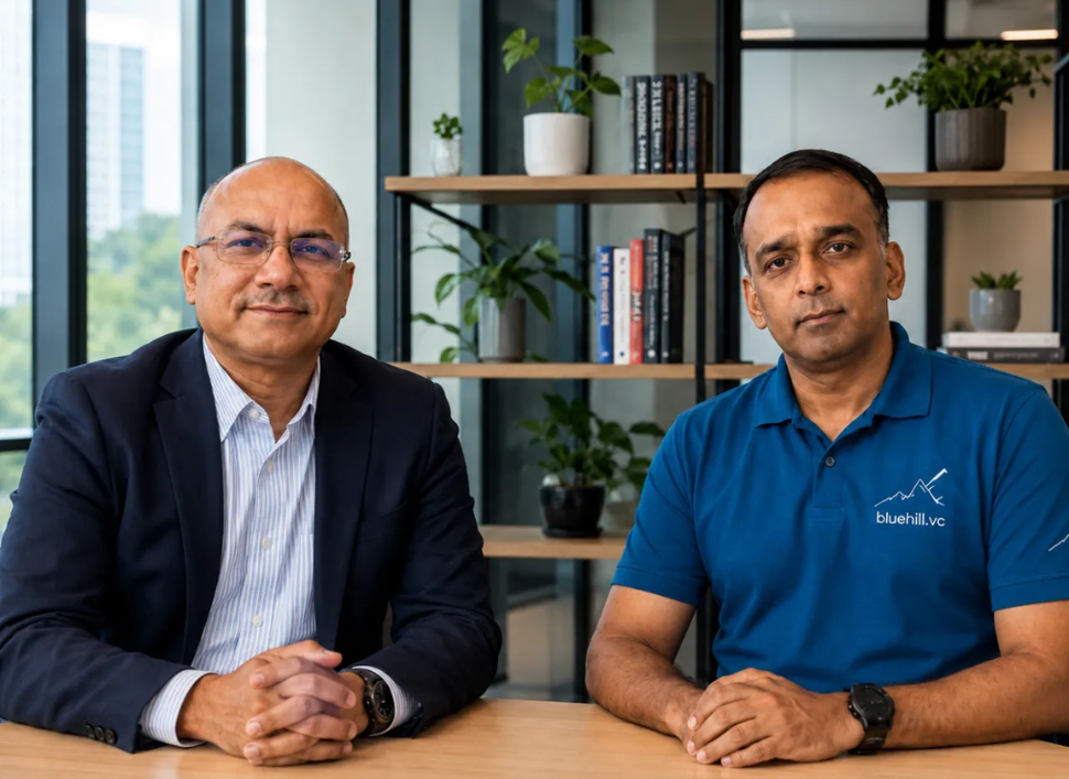
Semiconductor metrology startup Makr Microsystems has raised Rs 10.2 crore in a seed funding round led by Bluehill VC, with participation from Artha Venture Fund, to advance its non-destructive subsurface inspection technology for next-generation chip architectures.
Semiconductor metrology startup Makr Microsystems has raised Rs 10.2 crore in a seed funding round led by Bluehill VC, a venture capital firm focused on frontier technology. Artha Venture Fund also participated in the round.
The company said the newly raised capital will be used to further develop its technology, validate its product with customers and move closer to commercial deployment.
The funding comes as semiconductor manufacturing continues to shift toward increasingly complex architectures, including advanced packaging, chiplets and three-dimensional (3D) chip structures. These technologies rely on interfaces, interconnections and other structures located beneath multiple layers of material, making subsurface inspection increasingly important for manufacturers.
Being able to visualize and measure these hidden structures can help semiconductor manufacturers understand how devices have been constructed, identify defects and improve manufacturing yields.
Makr Develops Non-Destructive Subsurface Inspection Technology
Existing inspection and metrology technologies can provide detailed information about semiconductor structures, but manufacturers often face trade-offs involving resolution, inspection depth, measurement speed and whether the inspection process damages the sample.
Makr Microsystems is developing an approach intended to address these challenges through high-resolution, non-destructive subsurface measurement.
The company's core technology, Acoustic Atomic Force Microscopy (AAFM), combines atomic force microscopy (AFM) with acoustic sensing. The approach uses acoustic signals to obtain information from beneath a material's surface, addressing inspection requirements that conventional surface-based techniques may find difficult to resolve.
Makr is developing the technology as a platform for high-resolution, non-destructive inspection of structures beneath semiconductor surfaces. Its targeted applications include advanced packaging, hybrid bonding, buried interfaces, chiplet interconnects and defect detection.
The technology could be particularly relevant as semiconductor architectures increasingly move into the third dimension, where critical interfaces and connections can be difficult to inspect using conventional surface metrology approaches.
Focus on Advanced Semiconductor Packaging
Advanced packaging has become an increasingly important part of semiconductor manufacturing as chip designers seek higher performance and greater integration. Chiplets, hybrid bonding and 3D architectures can place critical connections and interfaces below the visible surface of a package.
For manufacturers, detecting defects in these structures without damaging the device can be important for process development, failure analysis and yield improvement.
Makr's AAFM technology is being developed around this requirement, with the company targeting inspection capabilities that combine high resolution with non-destructive subsurface measurement.
"Semiconductor manufacturing is creating structures that are increasingly difficult to see and measure. As architectures move into the third dimension, understanding what is happening beneath the surface becomes critical to improving yield. Our goal is to make the subsurface measurable, non-destructively and at the resolution the next generation of chipmaking demands," said founder Ashwin Lal.
Founder Brings Semiconductor Technology Experience
Ashwin Lal holds a Master's degree in Physics from IIT Kanpur and a PhD in Microtechnology from EPFL. He previously founded Shilps Sciences and worked as an engineer at Applied Materials.
His background in microtechnology and semiconductor-related engineering forms part of the technical foundation behind Makr Microsystems' development of AAFM for advanced semiconductor inspection and metrology applications.
The company is now focused on technology development and customer validation as it works toward commercial deployment.
Bluehill VC Sees Global Opportunity
Bluehill VC said Makr's technology addresses a challenging problem within the semiconductor manufacturing value chain, particularly as chip architectures become more complex.
Manu Iyer, General Partner at Bluehill VC, said, "We are excited about companies that sit deeper in critical technology value chains. Makr is solving a difficult problem in semiconductor manufacturing at a time when the industry is moving toward increasingly complex architectures. We believe this is a global opportunity, and that world-class semiconductor equipment and technology can be built from India."
The investment reflects growing interest in semiconductor equipment and deep-technology startups developing inspection and metrology solutions for advanced manufacturing.
With the new funding, Makr Microsystems plans to continue developing its AAFM platform, work with customers to validate the technology and progress toward commercial deployment.
As semiconductor manufacturers increasingly adopt advanced packaging, chiplets and 3D architectures, the ability to inspect structures beneath the surface without damaging devices is expected to remain an important requirement for process control, defect detection and yield improvement.