An international research team has achieved a major breakthrough in semiconductor metrology by developing a non-contact, non-destructive testing method capable of measuring shallow PN junction depths in silicon wafers with nanometer-scale resolution. The pioneering method uses femtosecond laser pulses to generate terahertz (THz) waves, enabling internal wafer inspection without damaging the material — a development that could transform quality control and reliability in next-generation 3D integrated semiconductor devices.
The research, published in Light: Science & Applications, is the result of a collaboration between Okayama University, Rice University, Samsung Japan Research Institute Group, and Samsung Electronics Group, led by Professor Masayoshi Tonouchi of Okayama University’s Research Institute for Interdisciplinary Science.
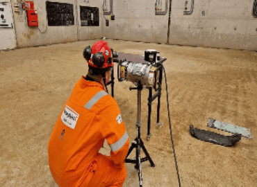
By illuminating silicon wafers with ultrashort femtosecond laser pulses, the researchers successfully excited photo-carriers at shallow PN junctions. These carriers, accelerated in opposite directions across the depletion region, emit THz radiation — which is then measured to determine the junction depth with exceptional accuracy. The system provides contactless electrical characterization without the need for invasive techniques like cutting or etching.
“The THz waves are essentially generated through the complicated ultrafast photocarrier behavior, but by employing the simple model of the behavior, one can understand the movement of the carriers intuitively and evaluate the depth of the PN junction. Here, we introduce the depth estimation procedure with the simple mode for the THz wave generation from PN junctions for the first time,” said Prof. Tonouchi.
The team also overcame a key challenge: optimizing laser penetration for shallow junction detection. “It was tricky to use shorter laser wavelengths to excite the shallow PN junctions of Si because the penetration depth of the typical femtosecond laser with a wavelength of around 800 nm is much longer than 10 micrometers for Si, and so, we cannot expect that the method is available to characterizing the shallow PN junctions in Si wafers at first,” explained Dr. Murakami, a young scientist on the team. “We found that a half wavelength is suitable in the present case, and by tuning the wavelength, one can evaluate shallower junctions more precisely.”
The new method comes at a critical juncture for the semiconductor industry, as chip manufacturers pursue smaller, faster, and more densely integrated designs. Current testing methods often fall short due to their inability to inspect buried features quickly and without causing damage.
“The complexity of semiconductor devices is accelerating as they aim for higher levels of integration, and the demands and issues for semiconductor wafer and device evaluation technology are increasing,” the researchers noted. “This technology, which enables rapid, non-destructive, and non-contact access to the interior of wafers… brings about an important innovation to solve this problem.”
The method is expected to improve wafer-level inspection, enhance device reliability, and reduce manufacturing waste and cost — critical advantages as the global semiconductor industry races to meet growing demand in AI, 5G, automotive, and high-performance computing sectors.