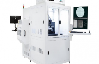
Confovis, a leader in innovative optical metrology, today unveiled IR-SIM (Infrared Structured Illumination Microscopy), a groundbreaking system designed to address the escalating demand for non-destructive inspection within complex bonded wafer stacks. This cutting-edge technology delivers precise, non-invasive analysis of hidden bond interfaces, overcoming a significant hurdle in the evolution of advanced semiconductor manufacturing.
Confovis has substantially expanded its metrology capabilities by advancing its patented Structured Illumination Microscopy (SIM) technology into the infrared spectrum. Operating at a wavelength of 1300nm, IR-SIM ingeniously renders silicon transparent, enabling unprecedented non-destructive imaging of internal structures within stacked or bonded wafers.
"IR-SIM extends our optical inspection capabilities into domains where other inspection and metrology systems come to their limits,” commented Frank Thielert, Business Development at Confovis. “It opens new possibilities for bonding metrology to see the root cause of voids and the analysis of buried structures in 2.5D/3D technologies and MEMS.”
The core innovation of IR-SIM lies in its ability to effectively "see through silicon." The system projects precisely phase-shifted patterns in the infrared range, then meticulously reconstructs the topography of the bonded interface from the modulated return signal. This sophisticated approach allows for thorough examination of the buried interface between two wafers—identifying voids, particles, or any other type of defect—all without compromising the device's integrity.
Frank Thielert further noted, “Early adopters report that IR-SIM gives additional information to scanning acoustic microscopy for interface defect detection, while delivering the quantitative metrology they need for statistical process control.”
Integrated seamlessly with the robust WAFERinspect platform, IR-SIM combines advanced 3D/2D metrology with AI-assisted defect inspection within a unified optical path. This powerful synergy empowers users to generate true-to-scale height maps of bond layer topography while simultaneously and automatically flagging defects crucial for statistical process control. The WAFERinspect series is distinguished by its unique area scanning Structured Illumination Microscopy approach, which provides high-precision, non-contact 3D measurements without the need for moving optical components. This integrated beam path also supports versatile image-based defect inspection using various light frequencies, ensuring exceptional flexibility, stability, repeatability, and accuracy for defect detection, classification, and dimensional measurement in advanced NDT applications.


